In this article, we'll take a technical examination of the technology behind graphics cards, their components, architecture, and how they relate to machine learning.
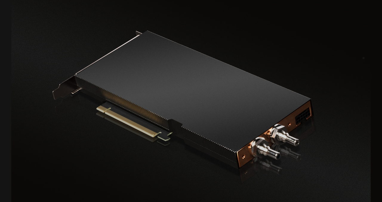
The task of a graphics card is very complex, yet its concepts and components are simple to comprehend. We will look at the essential components of a video card and what they accomplish. And at each stage, we'll use the NVIDIA A100 - 40 GB as an example of the current state of the art of graphics cards. The A100 arguably represents the best single GPU available for deep learning on the market.
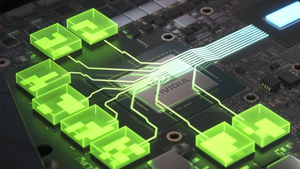
Graphics card breakdown
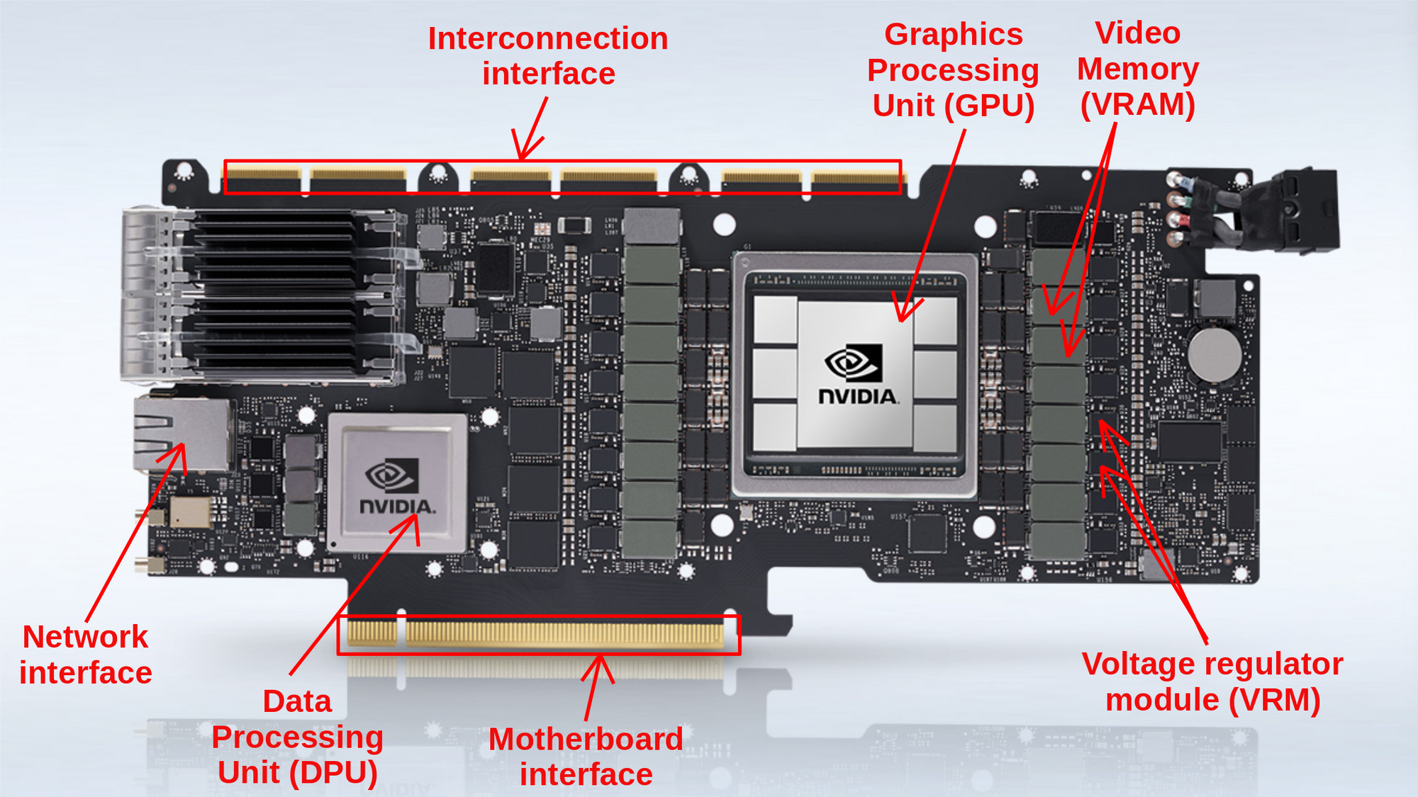
A graphics card, often known as a video card, graphics adapter, display card, or display adapter, is a type of expansion card that processes data and produces graphical output. As a result, it's commonly used for video editing, gaming, and 3D rendering. However, it's become the go-to powerhouse for machine learning applications and cryptocurrency mining in recent years. A graphics card accomplishes these highly demanding tasks with the help of the following components:
- Graphics Processing Unit (GPU)
- Data Processing Unit (DPU)
- Video Memory (VRAM)
- Video BIOS (VBIOS)
- Voltage regulator module (VRM)
- Motherboard interface
- Interconnection interface
- Network interface & controller
- Output Interfaces
- Cooling system
Graphics Processing Unit (GPU)
Frequently mistaken for the graphics card itself. The GPU, unlike a computer's CPU, is designed to handle more complex mathematical and geometric calculations required for graphics rendering. GPUs, on average, have more transistors and a larger density of computing cores with more Arithmetic Logic Units (ALU) than a normal CPU.
There are four classifications of these units:
- Streaming Multiprocessors (SMs)
- Load/Store (LD/ST) units
- Special Function Units (SFU)
- Texture Mapping Unit (TMU)
1) A Streaming Multiprocessor (SM) is a type of execution entity that consists of a collection of cores that share a register space, as well as shared memory and an L1 cache. Multiple threads can be simultaneously executed by a core in an SM. When it comes to SM's core, there are two major rivals:
- Compute Unified Device Architecture (CUDA) or Tensor cores by NVIDIA
- Stream Processors by AMD
NVIDIA's CUDA Cores and Tensor Cores, in general, are believed to be more stable and optimized, particularly for machine learning applications. CUDA cores have been present on every Nvidia GPU released in the last decade, but Tensor Cores are a newer addition. Tensor cores are much quicker than CUDA cores at computing. In fact, CUDA cores can only do one operation every clock cycle, but tensor cores can perform several operations per cycle. In terms of accuracy and processing speed, CUDA cores are not as powerful as Tensor cores for machine learning models, but for some applications they are more than enough. As a result, these are the best options for training machine learning models.

The performances of these cores are measured in the FLOPS unit (floating point operations per second). For these measurements, The NVIDIA A100 achieves record breaking values:
| Core | Specification |
|---|---|
| FP64 | 9.7 TFLOPS |
| FP64 Tensor Core | 19.5 TFLOPS |
| FP32 | 19.5 TFLOPS |
| FP32 Tensor Core | 156 TFLOPS |
| BFLOAT16 Tensor Core | 312 TFLOPS |
| FP16 Tensor Core | 312 TFLOPS |
| INT8 Tensor Core | 624 TFLOPS |
According the NVIDIA documentation, using sparsity format for data representation can even help double some of these values.
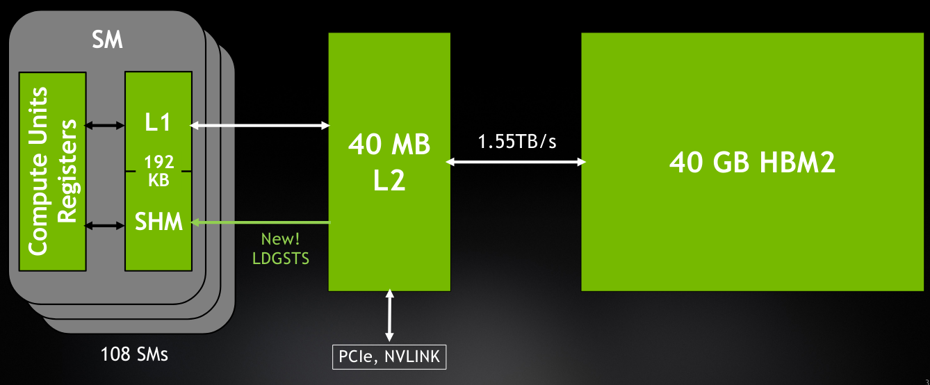
Inside the A100, cache management is done in a particular way to make data transfer between cores and VRAM as fast and smooth as possible. For this purpose, the A100 GPU has 3 levels of cache L0, L1 and L2:
The L0 instruction cache is private to a single streaming multiprocessor sub-processing block, the L1 instruction cache is private to an SM, and the L2 cache is unified, shared across all SMs, and reserved for both instruction and data. The L2 cache in the A100 is larger than all previous GPU's caches and comes with a size of 40MB and it acts as the bridge between the L1 private cache and the 40GB HBM2 VRAM which we will see in details later in this article.
2) Load/Store (LD/ST) units allow threads to perform multiple data loading and storing to memory operations per single clock cycle. In the A100, these unit introduce a new method for asynchronous copy of data, which gives the possibility to load data that can be shared globally between threads without consuming extra thread resources. This newly introduced method offers an increase of around 20% of data loading times between shared memory and local caches.
3) Special Function Units (SFUs) efficiently perform structured arithmetic or mathematical functions on vectored data, – for example sine, cosine, reciprocal, and square root.
4) Texture Mapping Unit (TMU) handles application-specific tasks such image rotation, resizing, adding distortion and noise, and moving 3D plane objects.
Data Processing Unit (DPU)
The DPU is a non-standard component of the graphics card. Data Processing units are a newly introduced class of programmable processor that joined CPUs and GPUs as the three main components of computing. So, a DPU is a stand-alone processor that is generally implemented in ML and Data centers. It offers a set of accelerated software abilities to manage: networking, storage, security. The A100 graphics card has on board the latest BlueField-2 DPU, which can give great advantages when it comes to handling workloads with massive multiple-input multiple-outputs (MIMO), AI-on-5G deployments, and even more specialized workloads such as signal processing or multi-node training.
Video Memory (VRAM)
In its broadest definition, video random-access memory (VRAM) is analogous to system RAM. VRAM is a sort of cache utilized by the GPU to hold massive amounts of data required for graphics or other applications. All data saved in VRAM is transitory. Traditional VRAM is frequently much faster than the system RAM. And, more importantly, it's physically close to the GPU. It's directly soldered to the graphics card's PCB. This enables remarkably fast data transport with minimal latency, allowing for high-resolution graphics rendering or deep learning model training.
On current graphics cards, VRAM comes in a variety of sizes, speeds, and bus widths. Currently, multiple technologies are implemented; GDDR and HMB have their own respective variations. GDDR (SGRAM Double Data Rate) has been the industry standard for more than a decade. It achieves high clock speeds, but at the expense of physical space and higher than average power consumption. On the other hand, HBM (High Bandwidth Memory) is the state of the art for VRAM technologies. It consumes less power and has the ability to be stacked to increase memory size while taking less real estate on the graphics card. It also allows higher bandwidth and lower clock speeds. The NVIDIA A100 is backed with the latest generation of HBM memories, the HBM2e with a size of 80GB, and a bandwidth up to 1935 GB/s. This is a 73% increase in comparison with the previous version Tesla V100.
Voltage regulator module (VRM)
It ensures that the GPU receives the necessary power at a constant voltage. A low-quality VRM can create a series of problems, including GPU shutdowns under stress, limited overclocking performances, and even shortened GPU lifespan. The graphics card receives 12 volts of electricity from a modern power supply unit (PSU). GPUs, on the other hand, are sensitive to voltage and cannot sustain that value. This is where the VRM comes into play. It reduces the 12-volt power supply to 1.1 volts before sending it to the GPU cores and memory. The power stage of the A100 with all its VRMs can sustain a power delivery up to 300 Watts.
Using the 8-Pin power connector the A100 receives power from the power supply unit, then forwards the current to the VRMs, that supplies the power to the GPU and DPU, as a 1.1 VDC current, rated at a maximum enforced limit of 300 W and a theoretical limit of 400 W.
Motherboard interface
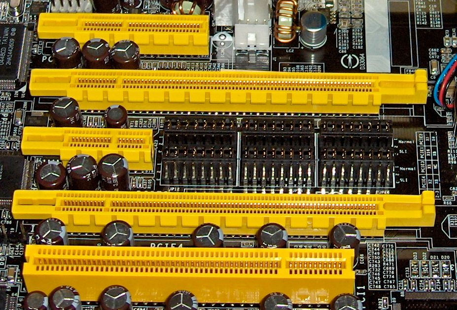
This is the sub-component of the graphics card that plugs into the system's motherboard. It is via this interface, or 'slot’, that the graphics card and the computer interchange data and control commands. At the start of the 2000s, many types of interfaces were implemented by different manufacturers: PCI, PCIe, PCI-X or AGP. But, now PCIe has become the go-to interface for mainly all graphics card manufacturers.
PCIe or PCI Express, short for Peripheral Component Interconnect Express, is the most common standardized motherboard interface for connection with graphics cards, hard disk drive, host adapters, SSDs, Wi-Fi and other Ethernet hardware connections.
PCIe standards have different generations, and by each generation there is a major increase in speed and bandwidth:
| Bandwidth | Gigatransfer | Frequency | |
|---|---|---|---|
| PCIe 1.0 | 8 GB/S | 2.5 GT/s | 2.5 GHz |
| PCIe 2.0 | 16 GB/S | 5 GT/s | 5 GHz |
| PCIe 3.0 | 32 GB/S | 8 GT/s | 8 GHz |
| PCIe 4.0 | 64 GB/S | 16 GT/s | 16 GHz |
PCIe slots can be implemented in different physical configurations: x1, x4, x8, x16, x32. The number represents how many lanes are implemented in the slot. The more lanes we have the higher bandwidth we can transfer between the graphics card and the motherboard. The NVidia A100 comes with a PCIe 4.0 x16 interface, which is the most performant commercially available generation of the interface.
Interconnection interface
The interconnection interface is a bus that gives system builders the possibility to connect multiple graphics cards mounted on a single motherboard, to allow scaling of the processing power through multiple cards. This multi-card scaling can be done through the PCIe bus on the motherboard or through a dedicated interconnection interface that acts as a data bridge. AMD and NVIDIA both present their graphics cards with proprietary methods of scaling, AMD with its CrossFireX technology and NVIDIA with its SLI technology. SLI was deprecated during the Turing generation with the introduction of NVLink, which is considered as the top of the line of multi-card scaling technologies.
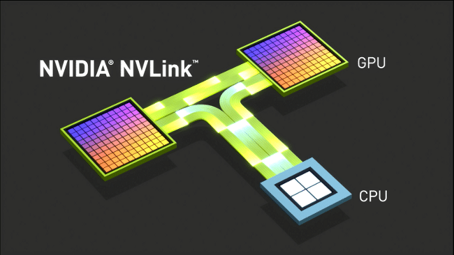
The NVIDIA A100 uses the 3rd generation of NVLink that can offer up to 600 GB/s speed between the two GPUs. Also, it represent a more energy efficient way, than PCI Express, to deliver data between GPUs.
Network interface
The network interface is not a standard component of the graphics card. It's only available for high performance cards that require direct data tunneling to its DPU and GPU. In the case of the A100, the network interface is comprised of 2x 100Gbps Ethernet ports that allows faster processing especially for applications involving AI-based networking.
Output Interfaces
The output interfaces are the ports that are built on the graphics card and gives it the ability to connect to a monitor. Multiple connection types can be implemented.
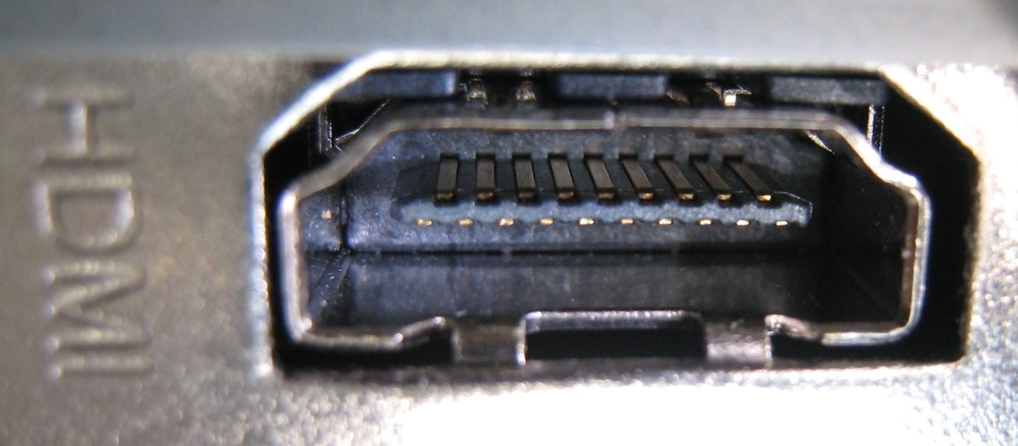
For older systems, VGA and DVI were used, while recently manufacturers tend to use HDMI and Display-Port while some portable systems implement the USB Type-C as the main port.
| HDMI | DisplayPort | DVI | VGA | |
|---|---|---|---|---|
| Digital or Analog | Digital | Digital | Digital | Digital |
| Speed | 340 Mhz | 165 MHz | 165 MHz | 28 MHz |
| Audio support | Yes | Yes | Yes | No |
| Max resolution | 7680 x 4320 px (8K) | 7680 x 4320 px (8K) | 3840 x 2400 px | 1920 x 1080 px |
As for the card under our microscope in this article, the A100 does not have an output interface. Since, it was designed from the start as professional card for ML/DL and use in data centers, so there is no reason for it have a display connectivity.
Video BIOS (VBIOS)
A video BIOS, often known as VBIOS, is a graphics card's Basic Input Output System (BIOS). The video BIOS, like the system BIOS, provides a set of video-related informations that programs can use to access the graphics card, as well as maintaining vendor-specific settings such as the card name, clock frequencies, VRAM types, voltages, and fan speed control parameters.
Cooling system
The cooling is generally not considered as a part of the graphics card components listing. But, due to its importance it cannot be neglected in this technical deep dive.
Due of the amount of energy consumed by graphics cards, a high amount of thermal energy is generated. And, to keep the performances during the activity of the card and to preserve the long term usability, core temperature values should be limited to ovoid thermal throttling which is the performance reduction due to high temperature at GPU and VRAM level.
For this, two techniques are mainly used: Air cooling and liquid cooling. We'll take a look at the liquid cooling method used by the A100.
The coolant enters the graphics cards through heat-conductive pipes and absorbs the heat when going through the system. Then, the coolant is pulled using liquid pumping toward the radiator that acts as a heat exchanger between the liquid in the pipes and the air surrounding the radiator. Cloud GPU services often come built in with tools to monitor this temperature, like Paperspace Gradient Notebook's monitoring tools. This helps prevent overheating if you are running particularly expensive programs by serving as a warning system.
How to measure the performance of a graphics card?
Now that we know the major components and parts of a graphics card, we will see how the performance of a given card can be measured so it can be compared to other cards.
To evaluate a graphics card two scheme can be followed: evaluate the technical specifications of the sub-components and compare them to the results of other cards, or perform a test (a.k.a a benchmark) on the cards and compare the scores.
Specifications based evaluation
Graphics card have tens of technical specifications that can help determine its performance. We'll list the most important ones to look for when making a choice based on this evaluation method:
Core counts: the number of cores on a GPU can be a good measurement to start with when looking at the potential performance of a card. However, this can give biased comparison when comparing GPUs with different core types and architectures.
Core speed: It indicates the number of individual elementary computations that cores perform every second, measured in MHz or GHz. Another measurement to look for when building a personal system is the overclock maximum core speed, which is generally much higher than the non-overclocked speed.
Memory Size: The more RAM a card have, the more data it can handle a given time. But, it does not mean that by increasing VRAM the performance will increase, since this also depends on other components that can bottleneck.
Memory type: Memory chips with the same size can present different performances based on the technology implemented. HBM, HBM2 and HBM2e memory chips perform generally better that GDDR5 and GDDR6.
Memory Bandwidth: Memory bandwidth can be viewed as a broader method for evaluating a graphics card's VRAM performance. Memory bandwidth is basically how quickly your card's VRAM can be accessed and used at any one time.
Thermal design power (TDP): It shows how much electricity is needed to produce the most heat that the cooling system is capable of handling. When building systems, TDP is an important element for evaluating the power needs of the card.
Benchmark based evaluation
While the technical specifications can offer a broad idea on where the graphics card stands in comparison with others, it does not give a definite quantifiable mean of comparison.
Enter the benchmark, which is a test that gives a quantifiable result that can be clearly comparable between cards. For machine learning oriented graphics cards, a logical benchmark would be an ML model that is trained and evaluated across the cards to be compared. On Paperspace, multiple DL model benchmarks (YOLOR, StyleGAN_XL and EfficientNet) were performed on all cards available on either Core or Gradient. And, for each one the completion time of the benchmark was the quantifiable variable used.
Spoiler alert! the A100 had the best results across all three benchmark test scenarios.
The advantage of the benchmark based evaluation is that it produces a single measurable element that can simply be used for comparison. Unlike the specification based evaluation, this method allows for a more complete evaluation of the graphics card as a unified system.
Why are graphics cards suitable for machine learning ?
In contrast to CPUs, GPUs are built from the ground up to process large amounts of data and carry out complicated tasks. Parallel computing is another benefit of GPUs. While CPU manufacturers strive for performance increases, which are recently starting to plateau, GPUs get around this by tailoring hardware and compute arrangements to a particular need. The Single Instruction, Multiple Data (SIMD) architecture used in this kind of parallel computing makes it possible to effectively spread workloads among GPU cores.
So, since the goal of machine learning is to enhance and improve the capabilities of algorithms, greater continuous data sets are required to be input. More data means these algorithms can learn from it more effectively and create more reliable models. Parallel computing capabilities, offered by graphics cards, can facilitate complex multi-step processes like deep learning algorithms and neural networks, in particular.
What are the best graphics cards for machine learning?
Short answer: The NVIDIA A100 - 80GB is the best single GPU available.
Long answer: Machine learning applications are a perfect match for the architecture of the NVIDIA A100 in particular and the Ampere series in general. Traffic moving to and from the DPU will be directly treated by the A100 GPU cores. This opens up a completely new class of networking and security applications that use AI, such as data leak detection, network performance optimization, and prediction.
While the A100 is the nuclear option when it comes to machine learning applications, more power does not always mean better. Depending on the ML model, the size of the dataset, the training and evaluation time constraints, sometimes a lower tier graphics card can be more than enough while keeping the cost as low as it can be. That's why having a cloud platform that offers a variety of graphics cards is important for an ML expert. For each mission, there is a perfect weapon.
Be sure to check out the Paperspace Cloud GPU comparison site to find the best deals available for the GPU you need! The A100 80 GB is currently only available in the cloud from Paperspace.
Resources
https://www.nvidia.com/en-us/data-center/a100/
https://developer.nvidia.com/blog/nvidia-ampere-architecture-in-depth/
https://www.nvidia.com/en-in/networking/products/data-processing-unit/


